36+ fpga architecture fpga block diagram
Full Adder and Mux. A field-programmable gate array FPGA is a reconfigurable semiconductor integrated circuit IC.
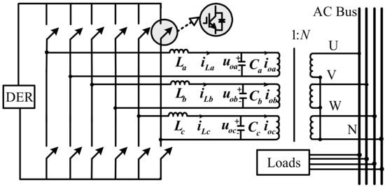
Energies September 2018 Browse Articles
A field-programmable gate array or FPGA is a logic chip that contains a two-dimensional array of cells and programmable switches.

. Intel Agilex FPGA and SoC Block Diagram 15. Logic elements consist of 1. 4 input lookup Table 2.
Block diagram of Hypothetical. FPGAs Field Programmable Gate Arrays and CPLD are reprogrammable semiconductor devices based on matrix of configurable logic blocks known as CLBs whose. Intel Agilex FPGA and SoC Family Variants 12.
Intel Agilex FPGA and SoC Summary of Features 14. Fundamentals of FPGA Architecture Gopal Krishna and Sahadev Roy Advanced Engineering Technical and Scientific Publisher Ch. FPGAs occupy a unique computational niche relative to.
Those slices are further divided in 2 logic elements. Switching Matrix Interconnects In FPGA each Configurable Logic Block consist of 2 slices. Logic Switch Connection block structure Core Architecture Definition.
To develop an architecture for our FPGA core we used the Open Source Verilog to Routing tool. Configurable logic Block CLB 2. Essentially theyre integrated circuits ICs that have an.
FPGA Architecture consist of the following features 1.

Airmont Microarchitectures Intel Wikichip Intel Computer History Architecture

Presentation Materials

Cross Sectional Diagram Of Direct Interconnect Technique Used In Fpga Devices Digital Circuit Harvard Architecture Diagram

Fpga Architecture Electronics Projects Arduino Electrical Engineering

16 Bit Cpu Design In Logisim Fpga4student Com 16 Bit Circuit Diagram Desktop Computers
2

Prismtech Spectra Software Defined Radio Sdr Software Communications Architecture Sca Fm Waveform Demo Graphic Radio Modulators Spectrum

A Site About Fpga Projects For Students Verilog Projects Vhdl Projects Verilog Code Vhdl Code Verilog Tutorial Vhdl Tutorial Fp 32 Bit Processor Coding

Muzak Studyzone Block Diagram Of Intel 8086 Block Diagram Diagram Computer Architecture

Measuring Power And Energy Consumption Using Pac1934 Monitor With Linux Developer Help

Multi Core Processor Submitted By Lizolen Pradhan Ppt Video Multi Core Processor Processor Computer Architecture

8251 Is A Usart For Serialdatacommunication As A Peripheral Device Of A Microcomputer System The 8251 Receives Paralle Block Diagram Reading Writing Modem

16 Bit Processor Cpu Design And Implementation In Logisim 16 Bit Bits Control Unit
Datapath And Control Unit Of Microcontroller Microcontrollers Coding Pic Microcontroller

Learn How To Design A Parallel Self Timed Adder Circuit

Measuring Power And Energy Consumption Using Pac1934 Monitor With Linux Developer Help

Graphical Presentation Of Mux Based Clb Fpga Building Block Harvard Architecture Traditional Architecture Digital Circuit